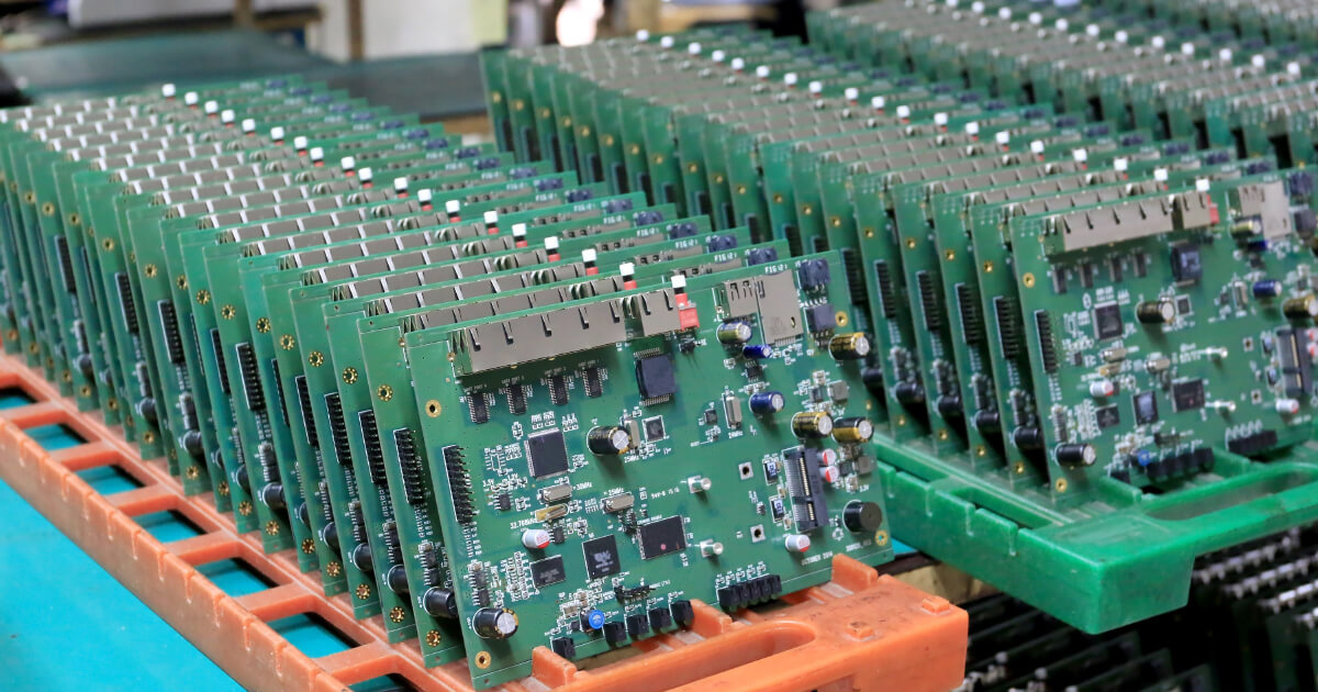
Printed Circuit Board (PCB) design is both a science and an art, and it could be a challenging and complex process that requires a deep understanding of electrical engineering principles, materials science, and manufacturing processes. It gets more interesting when you design an Automated Test Equipment (ATE) PCB. ATE PCB is widely used in functional and reliability testing of semiconductor chips (ICs), such as:-
- Microprocessors
- Memory chips
- System-on-a-Chip
- Graphical Processing Units
- Analog chips
- Power Management IC
The art of ATE PCB design involves balancing several competing factors to create a functional and efficient hardware to test the Device Under Test (DUT). So, herein in this blog, we will go through some of the factors you must consider while designing an ATE PCB.
Signal Integrity
Signal Integrity refers to the ability of electrical signals to maintain their quality and accuracy as they travel through the PCB. As ATE PCBs are meant to test Semiconductor chips, the quality of the PCB is paramount as it affects the accuracy and reliability of the test results. Factors like Trace impedance mismatch, Signal reflections, and Noise can affect the Signal Integrity. Best practices such as balanced PCB stack-up, tightly controlled impedance lines, good termination, and reducing via stubs can help to maintain the Signal Integrity.
Power Integrity:
Power Integrity refers to the stability and reliability of a PCB’s power delivery system. To test today’s low voltage and power-sensitive semiconductors, ATE PCBs need to be designed with a good Power Distribution Network (PDN). It plays a crucial role in ensuring stable voltage levels, reducing power noise and losses, and improving overall power efficiency. Solid power planes, optimized PCB stack-up, and De-coupling capacitor’s value and placement are crucial in ensuring good PDN design in ATE PCBs.
Mechanical Constraints:
ATE PCBs dock to a lot of equipment like Test head, Handler, Prober, etc. for high volume Automated IC testing. Each piece of equipment has its own Mechanical requirements which need to be addressed in the ATE PCB design. When the DUT is an RF device, cables, and their connectors need to be placed on the PCB, closer to the DUT, to connect to the RF test instruments. Adhering to these mechanical constraints eliminates PCB re-spin. ATE PCB designers work in tandem with Mechanical Engineers in defining placement constraints and validate the completed design for any violations.
Multi-Layered PCB:
The complexity and electrical requirements of the ATE PCBs call for a multi-layered structure. The high routing density and the need for dedicated layers for Power, Ground, and Signals increase the layer count to a Max. of 80 layers in the cases of a complex ATE PCB. Multi-layer PCBs have a tendency to warp when it undergoes the reflow soldering process. The PCB is made up of different types of materials: resin, glass fibers, and copper. Each material has its own thermal properties and when the PCB undergoes a thermal cycle the materials expand at a different rate causing PCB to warp. A balanced Multi-layer PCB helps to control the warpage within limits.
Via Technology:
Vias are small holes in a PCB that are used to connect different layers of the PCB together. As ATE PCBs are Multi-layered, vias are required by default. Choosing the right via technology is crucial for PCB manufacturing and performance.
- Through-hole vias: Through-hole vias are the most basic type of visa and are drilled through the entire PCB from one surface to the other. They are easy to manufacture and are suitable for larger-diameter vias; which is a disadvantage if you have fine pitch BGA (Ball Grid Array) DUT.
- Flip–drilled Through-hole vias: It’s the method of drilling Through-hole vias where the hole is drilled 50% of the way through from one side then the PCB is flipped over and the remaining hole is drilled from the other side. This helps when via drill size is small and the PCB thickness is high.
- Blind and Buried vias: Blind vias connect outer layers with inner layers and the Buried vias connect inner layers with inner layers only. A combination of these 2 vias, helps to fan out a fine-pitch BGA on much thicker ATE PCBs.
- Microvias: Microvias are laser-drilled vias used in HDI (High-Density Interconnect) PCBs. A micro via runs between 2 layers only and hence there is no stub and less inductive. This makes them the preferred choice for High data rate and RF signals routing.
Each technology has its advantages and limitations. The PCB designer needs to pick the right one for his/her design.
Conclusion
Designing ATE PCBs requires a combination of technical expertise in PCB layout, signal integrity, and power management, as well as an understanding of the specific requirements of the DUT and the ATE system. It’s a balance between technical knowledge, design skills, and creativity.
Tessolve PCB designers have mastered the ‘Art of ATE PCB Design’ with over 18 years of experience in delivering Quality ATE PCBs to test ICs from Top Semiconductor companies in the world. Our ATE designs have won the Best designs award from Siemens under the ‘Xcelerator Technology Innovation Awards program for 2020 and 2022.
To know more, connect with us today!
